UMC, a major wafer foundry, announced today the launch of a new 55nm BCD (Bipolar-CMOS-DMOS) platform to achieve higher power efficiency and system integration for next-generation mobile devices, consumer electronics, automotive and industrial applications.
UMC stated that this platform is designed to meet the increasingly complex power management requirements of electronic products, achieving smaller chip area, lower power consumption and excellent anti-noise performance, giving power circuit design greater flexibility and reliability.
UMC pointed out that BCD technology can integrate analog, digital and power components on a single chip and is widely used in power management and mixed-signal ICs. UMC's new 55nm BCD platform provides diversified power IC application solutions to meet the performance and reliability needs of different application fields, including:
Non-EPI process: A cost-effective solution with a unique component architecture that provides excellent power efficiency and performance for mobile and consumer devices. Epitaxy (EPI) process: complies with the most stringent automotive AEC-Q100 Grade 0 standard and supports operating voltages up to 150V, improving the reliability of automotive electronics in extreme environments. Silicon-on-insulation (SOI) process: It complies with the automotive AEC-Q100 Grade 1 standard. It has excellent anti-noise characteristics, high-speed operation and ultra-low leakage performance, and is very suitable for high-end automotive and industrial use. The platform also integrates ultra-thick metal layer (UTM), embedded flash memory (eFlash) and resistive random access memory (RRAM) technologies to further enhance chip performance and system integration flexibility.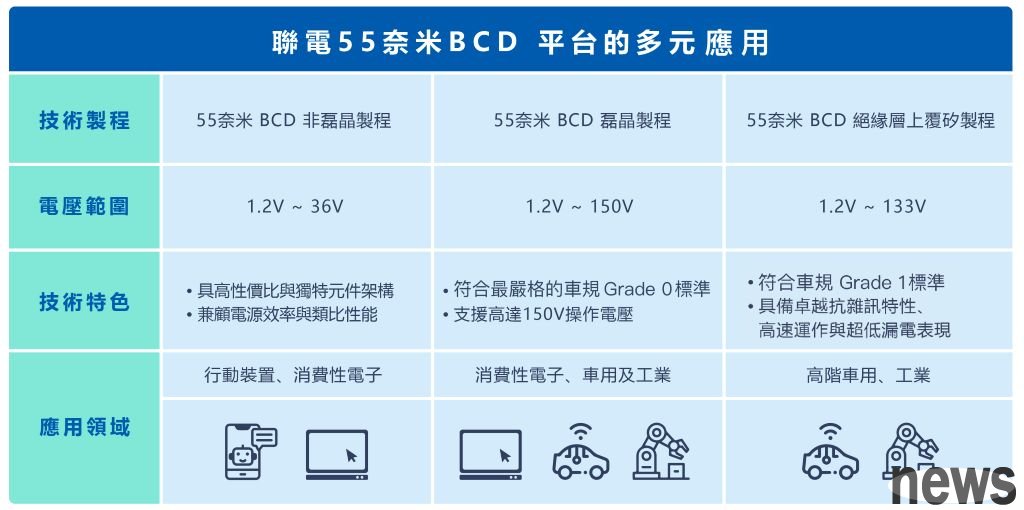 ▲ Diverse applications of UMC’s 55nm BCD platform.
Xu Shijie, deputy general manager of UMC Technology R&D, said that the launch of the 55nm BCD platform symbolizes an important milestone in UMC’s BCD technology layout. It will further improve our special process product portfolio and strengthen our competitive advantage in the power management market. Although the 55nm BCD process has been in mass production on the market for many years, UMC has launched a new and comprehensive 55nm BCD solution with excellent component characteristics to help customers create innovative power solutions. Its applications include smartphones, wearable devices, automotive, smart homes, smart factories and other fields.
UMC has built the industry's most complete and mature BCD technology portfolio, with process nodes spanning 0.35 micron, 0.25 micron, 0.18 micron, 0.11 micron and even 55 nanometers, providing differentiated solutions. By virtue of its ability to provide a wide range of voltage requirements, rich IP resources and complete design support, it accelerates customer product development processes, strengthens its competitiveness in the smart power and mixed signal markets, and continues to achieve long-term win-win growth with customers.