
Under the promotion of artificial intelligence (AI) and machine learning, global data flow is growing in multiples. At present, the connection between the data center server and the exchanger is rapidly moving from 200G and 400G to 800G and 1.6T, and may even reach the era of 3.2T.
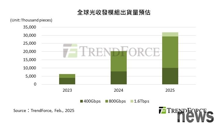
Market research organization TrendForce expects that the global shipment volume of optical harvest modules with a total of 400G or more in 2023 will be 6.4 million, about 20.4 million in 2024, and is expected to exceed 31.9 million by 2025, with an annual growth rate of 56.5%. Among them, the demand for AI servers continues to drive the growth of 800G and 1.6T, and traditional servers have also upgraded according to specifications, driving the demand for 400G optical transport modules.
According to a legal person, the demand for 1.6T optical modules in 2026 will significantly exceed expectations, with the total shipment expected to be as high as 11 million units, mainly from NVIDIA and Google's strong pull-out goods, as well as the proportion of Meta, Micro and AWS.
Due to the high frequency width, low consumption and long distance characteristics, optical communication has gradually become the main choice solution for the internal and external connection of the machine, making the optical harvesting module a key to the connection of the data center. TrendForce points out that in the future, data transmission between AI servers will require a large number of high-speed optical transmission modules that are responsible for converting the signal into optical signals, transmitting through optical standards, and converting the received optical signals back to the signal.
(Source: Cisco)
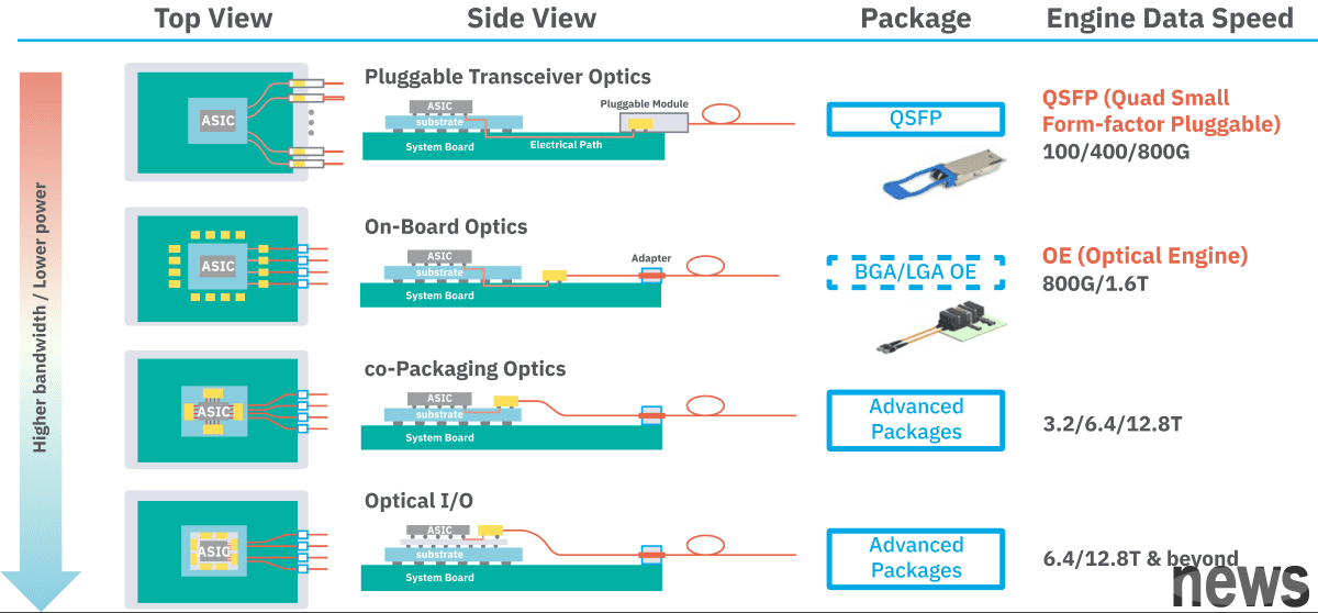
What is the relationship between optical transport modules, optical communications and silicon photons?From the first two diagrams below, we can see that the current pluggable optical receiver transmission rate on the market can reach 800G. The next stage optical engine (Optical Engine, simply OE) can be installed in the ASIC chip packaging area. This is called the board optical packaging (On-Board Optics, simply OBO), and its transmission capacity can support 1.6T.
(Source: Sun and Moonlight)
At present, the industry hopes to move towards "CPO" (Co-packaged Optics), that is, optical components and ASICs can be jointly packaged. Through this technology, it can actually exceed 3.2T and reach a transmission speed of 12.8T; the ultimate goal is to achieve "Optical I/O" (optical I/O), which realizes technologies similar to all-optical networks, and promotes transmission speeds of more than 12.8T.
If you look carefully at the above map, you can find that the optical communication module (formerly pluggable) that is used as a yellow square is getting closer to the ASIC, mainly to shorten the transmission path of the signal and achieve a higher frequency width. Silicon photon processing technology is the technology of integrating optical components into chips.
{twenty four}(Source: Sun and Moonlight)
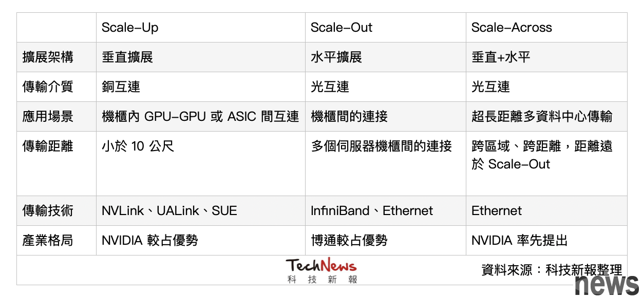
The demand for optical communications has skyrocketed, and the industry focuses on three expansion server architecturesDue to the huge explosion in AI applications, the demand for high-speed optical communication has increased sharply. Currently, servers mainly focus on two expansion directions: Scale Up (vertical expansion) and Scale Out (horizontal expansion), which are different transmission needs and technical challenges. Recently, NVIDIA has announced the concept of "Scale Across", adding a thinking direction to the industry.
Scale-Up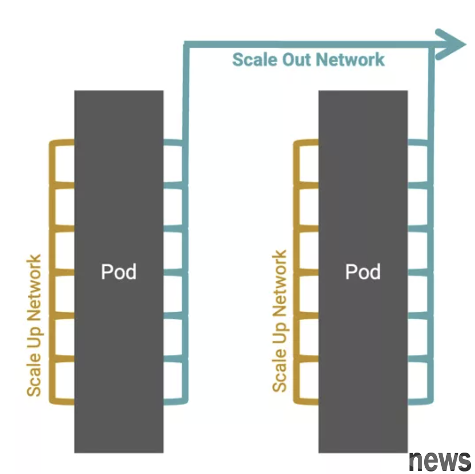
(Source: Synopsys Technology)
Scale-Up is mainly used as a high-speed interconnect (the yellow part of the picture above), and the transmission distance is usually within 10 meters. Due to the extremely low requirements for delay, the internal use of "Copper Interconnects" is still mainly used to avoid delay and energy consumption caused by optical conversion. Currently, the solutions are mainly NVIDIA's NVLink (closed architecture) and UALink (open architecture) led by AMD and other companies.
Interestingly, this year NVIDIA launched NVLink Fusion, opening NVLink technology to external chip manufacturers for the first time, extending NVLink from a single server stage to the entire Rack-Scale architecture. It is not ruled out that it is due to UALink's competition.
Another thing worth noting is that Broadcom, which was originally focused on Scale-Out, is trying to enter the Scale-Up market through the "Ethernet". The company recently launched a number of Scale-Up chips that are available for Scale-Up Ethernet standards, and this part can be seen later on the competition between NVIDIA and Broadcom.
Scale-OutScale-Out is a large-scale parallel computing across servers (the blue part in the picture above), which can understand the high throughput of the data and achieve infinite expansion. This is mainly based on "optical communication". The main network interconnection technology needs to rely on InfiniBand or Ethernet, which will also drive the optical communication module market.
InfiniBand and Ethernet can be divided into two major enterprises. The former is more popular among major factories such as NVIDIA and Microsoft, while the latter is mainly based on Broadcom, Google and AWS..
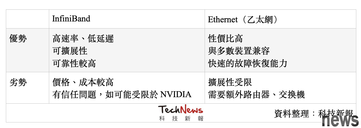
When talking about InfiniBand, we have to mention the leader manufacturer Mellanox, who was purchased by NVIDIA in 2019, mainly providing end-to-end Ethernet and InfiniBand smart interconnected solutions providers. China recently ruled that NVIDIA violated the anti-corruption law, which is to target this purchase case. Another point of concern is that although NVIDIA has launched many InfiniBand products, it also launched related products such as NVIDIA Spectrum-X for Ethernet, which can be said to be a two-market food.
Being another major enterprise, including Intel, AMD, Broadcom and other major factories, was organized to form the "Ultra Ethernet Consortium" (simplified by UEC) in July 2023. The cooperation to develop and improve the improved Ethernet Transfer Architecture has become one of the forces challenging InfiniBand.
TrendForce analysts believe that the optical communication module market led by Scale Out is the core battleground for future data transmission.
Scale-Across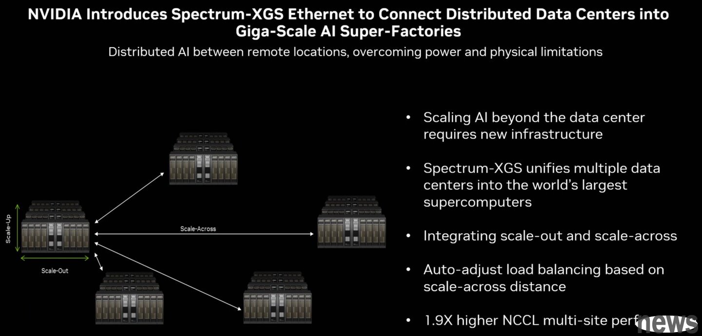
(Source: NVIDIA)
As a new solution, NVIDIA recently proposed the concept of "Scale-Across", namely "far distance connection" across data centers, with a distance of more than several kilometers, and has launched the Spectrum-XGS ether network based on the ether network and connected to multiple data centers.
Spectrum-XGS Aether Network will be regarded as the third pillar outside Scale-Up and Scale-Out. It is mainly used to expand the ultimate performance and scale of Spectrum-X Aether Network, and can connect to multiple decentralized data centers. According to NVIDIA, the NVIDIA Spectrum-X ethernet not only provides the Scale-Out architecture, but also connects the entire set and connects multiple distributed data centers to quickly stream large sets of data to the AI model. It can also coordinate communication between the GPU and the GPU within the data center.
In other words, this solution combines Scale-Out with cross-domain expansion, and can flexibly adjust load balance and dynamic adjustment algorithms based on cross-domain distance, so the concept is more similar to "Scale-Across".
NVIDIA founder and executive director Huang Rensheng said, "We have further joined Scale-Across in line with Scale-Up and Scale-Out capabilities, connecting data centers across cities, countries and even across continents to create a large super AI factory."
If we look at the current industry trend, Scale-Up and Scale-Out are both must-fight places, and we can see how NVIDIA and Broadcom can get a point in their own territory. The newly-announced Scale-Across by NVIDIA focuses on the transmission of cross-data centers across kilometers and even thousands of kilometers. Interestingly, Broadcom has also launched related solutions. For details, please see the next article: "AI chip transfer to CPO positioning battle: What are NVIDIA and Broadcom competing? (Part 2)》