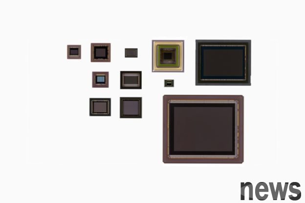
Sony's next-generation CMOS image sensors used in smartphones will be shipped in 2029 and will use a 3-layer structure, 22-28 nanometers (nm) process.
News reported on the 9th that Sony Semiconductor Solutions (hereinafter referred to as Sony Semiconductor) president of Sony's subsidiary, said that the next-generation CMOS image sensor used on smartphones will be shipped in 2029. The next-generation CMOS sensor developed by Sony Semiconductor will use a 3-layer structure (currently acting as 2-layer), a 22-28 nanometer process (currently acting as 40 nanometers), so as to improve sensitivity, resolution, reading speed and other performance without changing size.
report pointed out that although Sony's semiconductor CMOS image sensor ranks the highest global market share, it still cannot be stable. Samsung Electronics is a rival to Sony's semiconductor CMOS sensor, and Sony's large customer Apple previously stated that Samsung will supply chips for Apple devices including iPhones in Texas chip factories.
However, Tian Shinji pointed out with confidence, "As of around 2029, the business negotiations have been roughly completed. The focus is after 2030. As long as the technology in the current plan can be completed, the existing business can be maintained."
According to Yahoo Finance's price report, as of 12:20 am on the 10th, Sony rose 1.87% to 4,296 days round, and the highest was 4,307 days round, and the listing of the brand-name brand was a record high.
Taiwan Electric's factory (Kumamoto Ichi) located in Kikumachi, Kumamoto Prefecture, Japan has mass-produced and produced 12-28 nanometer process logic chips by the end of 2024. Kumamoto Factory is responsible for operation by Japan Advanced Semiconductor Manufacturing (JASM), a subsidiary of the crystal foundry service in Kumamoto Prefecture, while Sony semiconductors provide investments in JASM.